WATANABE Takanobu
WATANABE Takanobu
Dept. of Electronics and Physical Systems Dept. of Nanoscience and Nanoengineering
Specialization:Electron/electric material engineering, Mathematical physics/fundamental theory of physical properties, Nano structural science
Education
1995 B.E. degree in Electronics and Communication Engineering, Waseda University
1997 M.E. degree in Electronics, Information and Communication Engineering, Waseda University.
1999 Ph.D. degree in Electronics, Information and Communication Engineering, Waseda University. (Ph.D.Eng.)
Career
1997-2003 Japan Society for Promotion of Science, Research Fellow.
2003-2005 Lecturer, Graduate School of Science and Engineering, Waseda University.
2003-2007 PRESTO Researcher, Japan Science and Technology Agency
2005- Associate Professor, Graduate School of Science and Engineering, Waseda University. (Present)
2006 Visiting Professor, University of Southern California, U.S.A.
Research
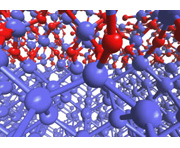
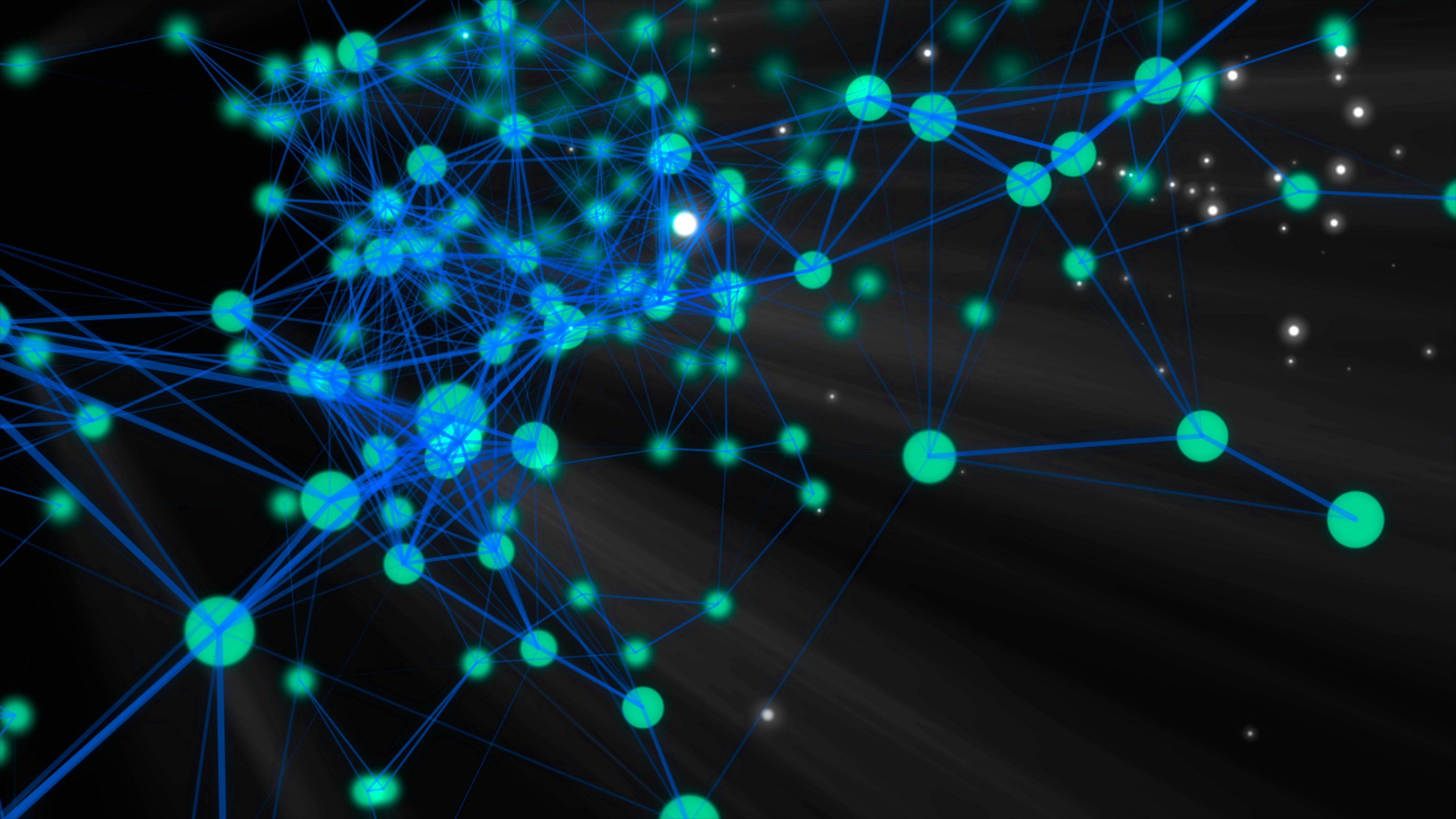
We are studying the physics and chemistry of semiconductor surfaces and interfaces by means of our original large-scale atomistic simulation techniques. We are also planning to start experimental studies on the surface processes with scanning tunneling microscopy. Our research interest is oriented toward basic condensed-matter physics, but we focus on the important issues in the application of forefront semiconductor electronics. Nowadays, wide range of elements in the periodic table is surveyed in microelectronics, so that a further powerful atomistic simulation method is required to boost the material designing. The development of such a new, highly transferable atomistic simulation technique is one of main targets of our researches.