
KAWAMURA Kazushi

KAWAMURA Kazushi
Dept. of Electronics and Physical Systems
Specialization:Intelligent processing systems
Education
2012, B. Eng. degree, Department of Computer Science and Engineering, School of Fundamental Science and Engineering, Waseda University
2013, M. Eng. degree, Department of Computer Science and Engineering, Graduate School of Fundamental Science and Engineering, Waseda University
2016, Dr. Eng. degree, Department of Computer Science and Engineering, Graduate School of Fundamental Science and Engineering, Waseda University
Career
2015–2016, Research Fellow (DC2), Japan Society for the Promotion of Science (JSPS)
2016–2017, Research Fellow (PD), Japan Society for the Promotion of Science (JSPS)
2017–2018, Junior Researcher (Assistant Professor), Waseda Research Institute for Science and Engineering
2018–2020, Assistant Professor (without tenure), Faculty of Science and Engineering, Waseda University
2020–2025, Specially Appointed Assistant Professor, Institute of Innovative Research, Tokyo Institute of Technology (From October 2024, Institute of Integrated Research, Institute of Science Tokyo)
2020–2025, Adjunct Researcher, Green Computing Systems Research Organization, Waseda University
2025–, Assistant Professor, Faculty of Science and Engineering, Waseda University
Research
The rapid advancement of artificial intelligence (AI) has brought us into an era where large-scale and complex social issues can be addressed through AI technologies. In response to this shift, we are engaged in research on computing platforms that can efficiently execute AI workloads, as well as intelligent processing systems built upon these platforms. The requirements for intelligent systems vary depending on the social problems to be solved. Therefore, it is essential to take a holistic approach that spans applications, algorithms, and hardware architectures, while keeping the final system design in mind. Currently, we are exploring flexible and efficient approaches to intelligent system design in the domain of combinatorial optimization and machine learning.
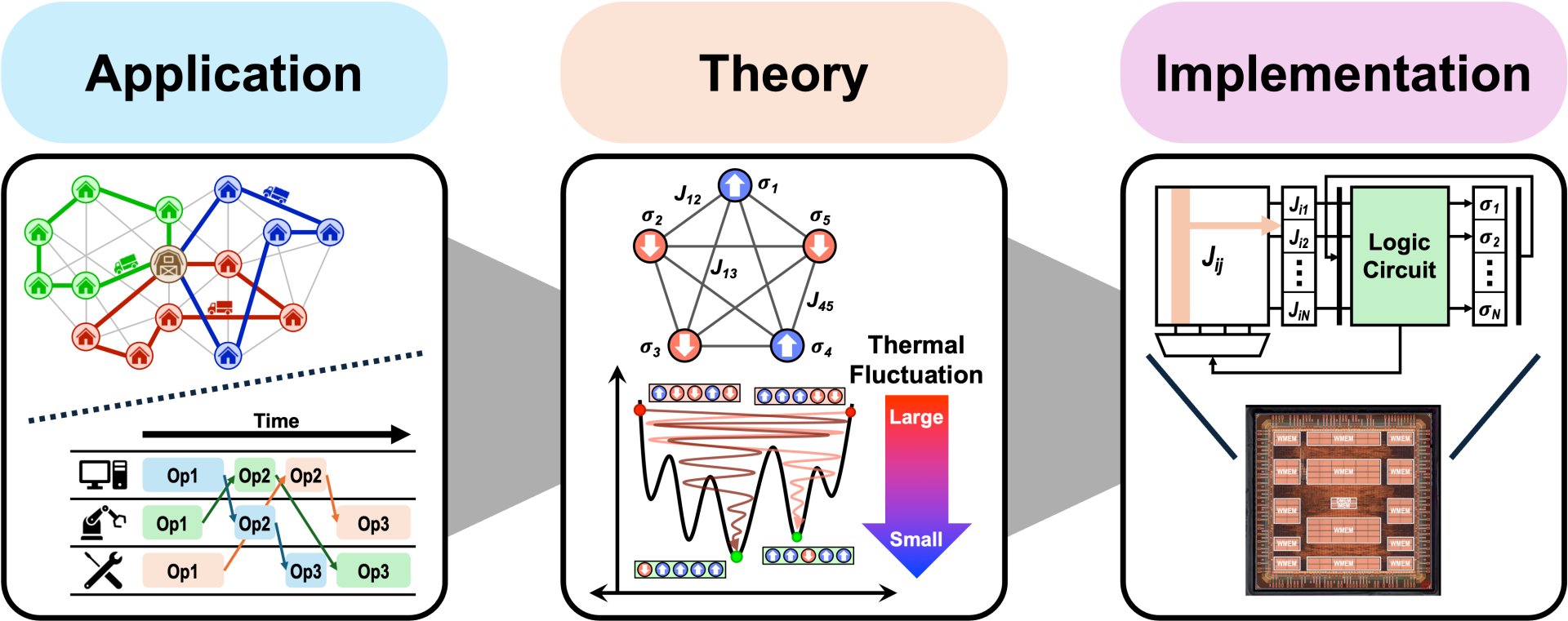
Towards comprehensive research on intelligent processing systems: from theory and implementation to practical applications